
Resource / Structural Redesign Record
How is a standard PCBA reorganized into a thin cold-pressed card?
The board is not simply placed inside a card. Battery, buzzer, antenna, button, component height, and test points must be reorganized as a finished-product stack.
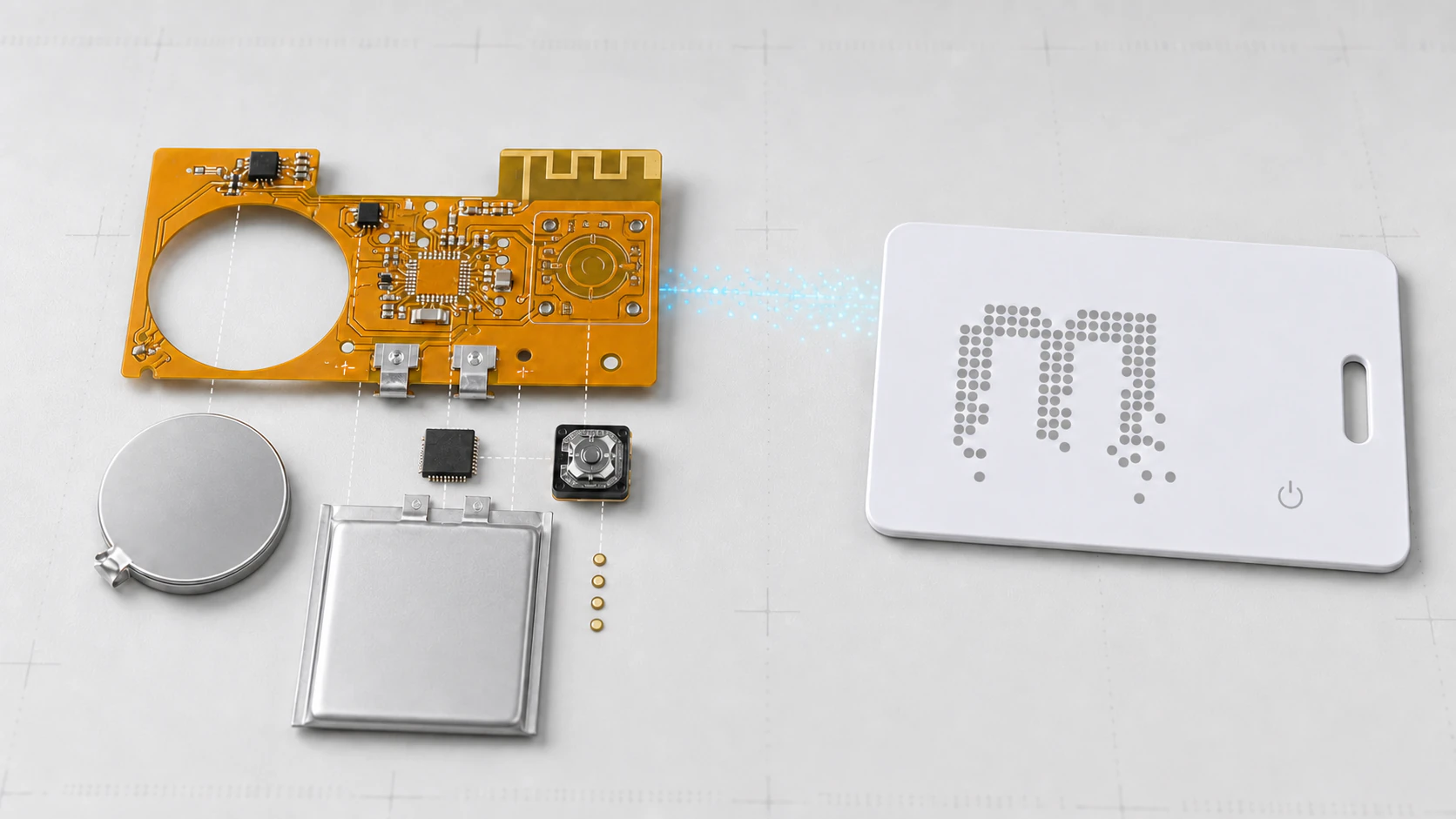
Evidence Baseline
Confirm real components before designing the card body.
The standard PCBA material shows the flexible circuit, controller and peripheral parts, BLE antenna zone, round buzzer, 3.0 V 540 mAh thin battery, and connection points. The white sample provides the finished-card form, button, and local opening reference.
Structural Redesign
Six structural actions turn the board into a cold-pressed smart card.
Each action affects thickness, appearance, wireless behavior, acoustics, and production testing, so no module can be designed in isolation.
- 01
Map component height
Record local height for ICs, buzzer, battery connection, button, and test points to identify surface-protrusion risks.
- 02
Rearrange battery and board
Lay the thin battery and main circuit region as flat as possible to reduce stacked Z-height peaks.
- 03
Preserve BLE clearance
Keep battery, copper, encapsulant change, and face materials from compromising the antenna zone; retest RF before and after pressing.
- 04
Build the buzzer cavity
Buzzer disc, support, sound opening, and encapsulant keep-out jointly define SPL; bare-component sound is insufficient.
- 05
Define button and opening
Button placement balances feel, graphics, local support, and protection; openings follow actual component location.
- 06
Plan filling and tests
Define encapsulant flow, venting, edge sealing, and fixtures while retaining functional, power, RF, and acoustic records.
Before and After
The redesign changes product structure, not its functional definition.
Controller, BLE, buzzer, button, and power functions remain corresponding. Structural redesign resolves placement, protection, interaction, and test access in the thin body.
| Object | Board state | Cold-pressed card requirement | Validation |
|---|---|---|---|
| PCBA | Function and electrical connection | Height, filling, support, and test points | Function, power, appearance |
| Battery | 3.0 V / 540 mAh | Flat placement, protected connection, edge margin | Voltage, resistance, load, safety |
| BLE | Board antenna zone | Finished-product clearance, face sheet, encapsulant | RSSI / PER / link |
| Buzzer | Disc and drive | Cavity, opening, support, keep-out | dB(A) / sound quality |
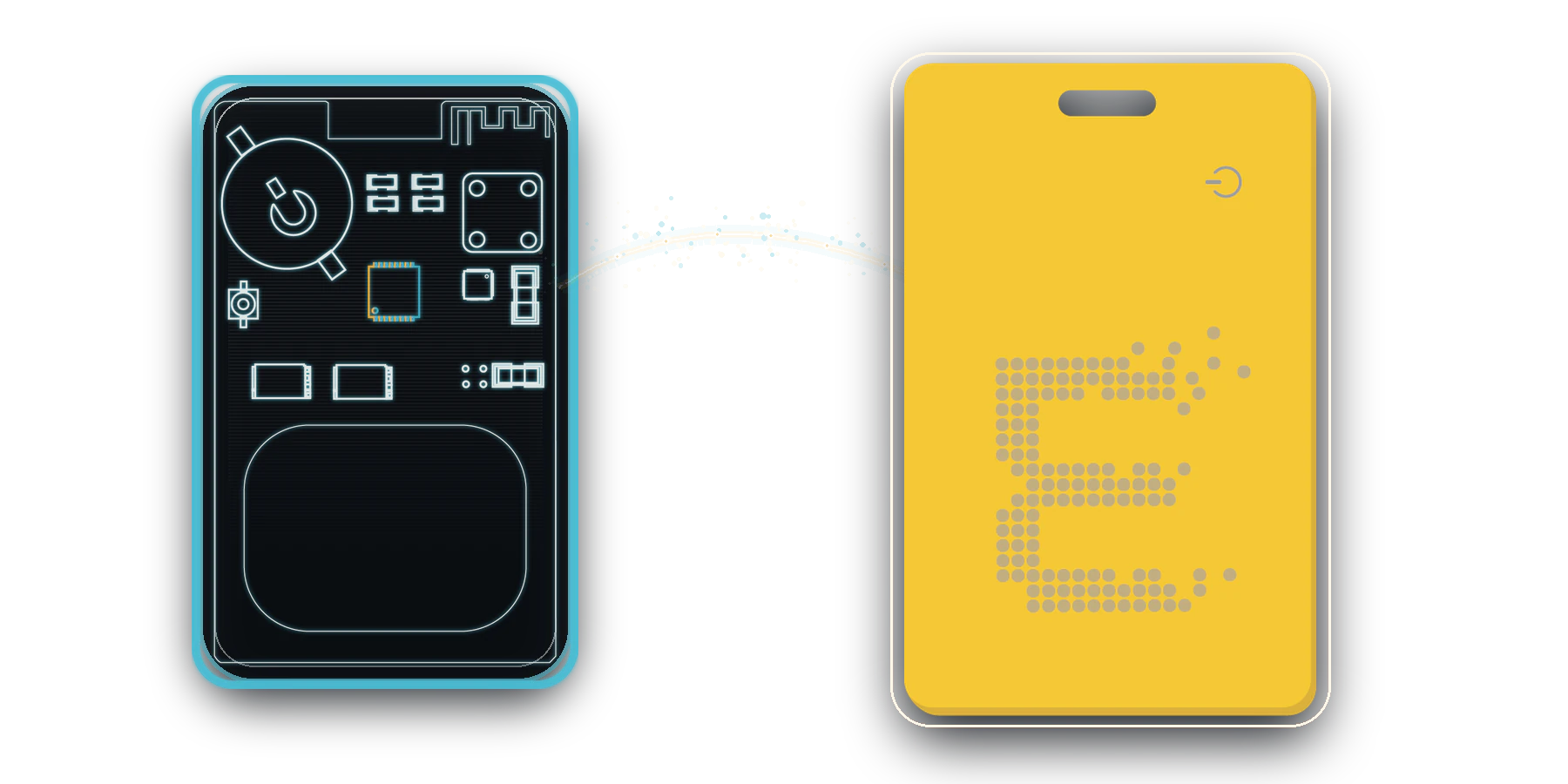
Validation Gate
The redesign enters validation only after the sample becomes a card.
Validate thickness and warpage, button feel, buzzer SPL, BLE link, standby power, battery connection, appearance consistency, and edge sealing. Add NFC, e-paper, or sensor tests when those modules are included.
Review cold-press structure with the real project board.
Provide PCB/PCBA drawings, component height, battery, antenna zone, buzzer, and target card body so Yuli can review stack-up, prototypes, tests, and production transfer.